Researchers from the National Institute of Standards and Technology (NIST) and Seoul National University (SNU) have learned how to tweak a new class of polymer-based semiconductors to better control the location and alignment of the components of the blend.
Their recent results—how to move the top to the bottom—could enable the design of practical, large-scale manufacturing techniques for a wide range of printable, flexible electronic displays and other devices.
Organic semiconductors—novel carbon-based molecules that have similar electrical properties to more conventional semiconducting materials like silicon and germanium—are a hot research topic because practical, high-performance organic semiconductors would open up whole new categories of futuristic electronic devices. Think of tabloid-sized “digital paper” that you could fold up into your pocket or huge sheets of photovoltaic cells that are dirt cheap because they’re manufactured by—basically—ink-jet printing.
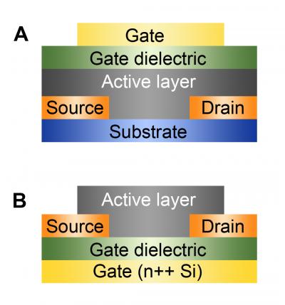
The problem is performance. Small organic molecules have been developed with key electrical parameters close to the benchmark set by amorphous silicon semiconductors, but they are very difficult to deposit in a stable, uniform film—a key manufacturing requirement. Larger molecule polymer semiconductors, on the other hand, make excellent thin films but have at best limited semiconductor properties. A patent from British researchers in 2005 offered a promising compromise: blend the small semiconductor molecules in with the polymer. This works surprisingly well, but with an asterisk. Tests showed that actual devices, field effect transistors, made with the blend only worked well in a so-called “top-gated” structure. The critical active part of the film was on the top, and the switching part of the device (the “gate”) had to be layered on top of that, a process difficult or impossible to do on a large scale without destroying the fragile film.
Working at NIST’s Center for Neutron Research, the SNU/NIST research team used a neutron imaging technique that allowed them to observe, with nanometer resolution, how the distribution of small organic semiconductor molecules embedded in polymer films changed with depth—the films are less than 100 nanometers thick. In the thin films originally described by the patent, the bulk of the semiconductor molecules end up at the top of the film, as suspected. However, when the SNU/NIST research team substituted a polymer with significantly higher molecular mass, something interesting happened. The organic semiconductor small molecules distributed themselves evenly at the top and bottom of the film. Having an active region of the film on the bottom is key for large-scale manufacturing because it means the rest of the device—gate, source, drain—can be laid down first and the delicate film layer added last.
In addition, they report, the optimized blend of polymer and organic semiconductor actually has better performance characteristics than the organic semiconductor on its own.
Article: J. Kang, N. Shin, D.Y. Jang, V.M. Prabhu and D.Y. Yoon. Structure and properties of small molecule-polymer blend semiconductors for organic thin film transistors. Journal of the American Chemical Society, Published on the Web Aug. 23, 2008.